
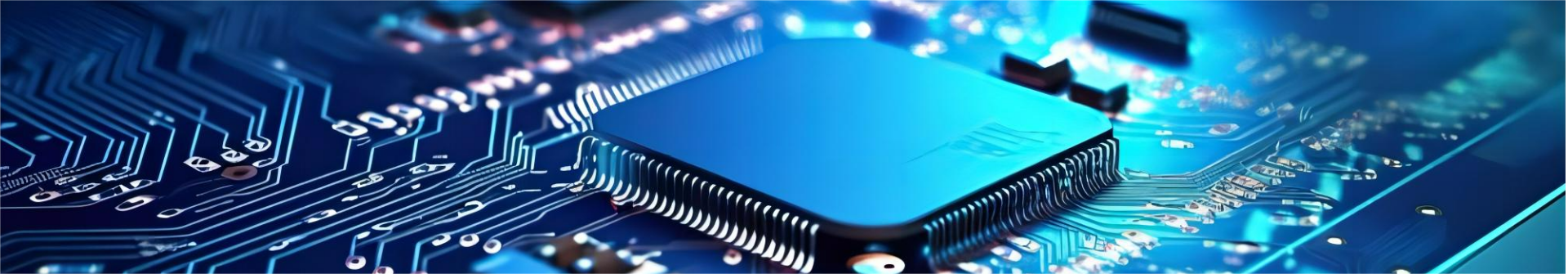
An Integrated Circuit (IC) Chip, often simply called a "microchip," is a miniaturized electronic circuit that integrates thousands, millions, or even billions of electronic components—such as transistors, diodes, resistors, and capacitors—onto a single, tiny semiconductor material (typically silicon). This revolutionary technology replaced the bulky, unreliable discrete circuits of the mid-20th century, enabling the miniaturization, cost reduction, and performance enhancement of nearly all modern electronic devices.

1. Core Function of IC Chips
At its essence, an IC chip processes electrical signals and manages power flow to perform specific tasks in electronic systems. Its core roles can be categorized into three key functions:
a. Signal Processing
ICs manipulate electrical signals (analog or digital) to transmit, convert, or refine information. For example:
Analog ICs (e.g., operational amplifiers, sensors): Convert physical inputs (light, sound, temperature) into continuous electrical signals and amplify/filter these signals. A microphone’s IC, for instance, turns sound waves into amplified electrical signals for a speaker.
Digital ICs (e.g., microprocessors, logic gates): Process discrete, binary signals (0s and 1s) to execute calculations, store data, or run programs. The CPU (Central Processing Unit) of a computer—an advanced digital IC—performs billions of binary operations per second to run software.
b. Data Storage
Specialized ICs, known as memory chips, store digital data temporarily or permanently:
Volatile memory (e.g., DRAM): Loses data when power is off; used for a computer’s "working memory" (RAM) to quickly access data for active tasks.
Non-volatile memory (e.g., Flash, ROM): Retains data without power; used in smartphones (for app storage), USB drives, and BIOS chips (to boot computers).
c. Power Management
Power Management ICs (PMICs) regulate, distribute, and convert electrical power to match the needs of different components in a device. For example, a smartphone’s PMIC converts the battery’s 3.7V output to lower voltages (e.g., 1.2V for the CPU, 3.3V for the display) to prevent component damage and save energy.
2. Key Characteristics of IC Chips
IC chips stand out from traditional discrete circuits due to several defining features, which underpin their widespread use:
a. Miniaturization
Size: Most ICs range from a few millimeters (mm) to around 30mm in length/width (e.g., a smartphone’s CPU is ~10mm x 10mm). The semiconductor material (silicon wafer) is sliced into thin "dies" (the core of the IC), with components etched onto the die using nanoscale manufacturing (current leading processes use 3nm–7nm technology, meaning transistor sizes are just a few nanometers wide).
Impact: Enables portable devices (smartphones, laptops, wearables) that would be impossible with bulky discrete circuits.
b. High Reliability
Reduced Interconnections: Discrete circuits rely on thousands of external wires to connect components, which are prone to damage, corrosion, or loose connections. ICs integrate all components and their connections onto a single silicon die, eliminating most external wiring.
Consistency: Manufacturing processes (e.g., photolithography) produce ICs with uniform component quality, reducing failure rates. Modern ICs have a mean time between failures (MTBF) of decades in many applications.
c. Low Power Consumption
Efficient Design: Nanoscale transistors (e.g., 3nm) require far less voltage and current to switch on/off compared to larger discrete components. For example, a single transistor in a 7nm IC uses ~0.7V, while a 1970s discrete transistor might use 5V–12V.
Impact: Critical for battery-powered devices (smartphones, IoT sensors) that need to operate for hours or days on a single charge.
d. High Performance & Speed
Fast Signal Transmission: Components on an IC are spaced just nanometers apart, so electrical signals travel much shorter distances than in discrete circuits. This reduces "propagation delay" (time for signals to move between components).
Parallel Processing: Advanced ICs (e.g., CPUs, GPUs) contain billions of transistors that can execute multiple tasks simultaneously. A modern GPU, for example, can perform trillions of floating-point operations per second (TFLOPS) for gaming or AI.
e. Cost-Effectiveness
Mass Production: ICs are manufactured in bulk on silicon wafers (typically 12-inch/300mm diameter wafers, each holding hundreds of IC dies). This economies-of-scale drives down per-unit costs.
Reduced Assembly: Unlike discrete circuits, which require manual or automated assembly of individual components, ICs are pre-integrated—simplifying device manufacturing and cutting labor costs.
3. Common Types of IC Chips
ICs are classified based on their complexity (number of components) and function. Below are the most widely used categories:
|
Type of IC |
Complexity (Components) |
Key Examples |
Typical Applications |
|
SSI (Small-Scale Integration) |
< 100 |
Logic gates (AND, OR, NOT), flip-flops |
Simple circuits (calculators, basic controllers) |
|
MSI (Medium-Scale Integration) |
100–10,000 |
Counters, multiplexers, decoders |
Digital clocks, traffic lights, washing machine controllers |
|
LSI (Large-Scale Integration) |
10,000–100,000 |
Early microprocessors, memory chips (RAM) |
1980s computers, early game consoles |
|
VLSI (Very-Large-Scale Integration) |
100,000–1 billion |
Modern CPUs, GPUs, microcontrollers |
Laptops, smartphones, gaming consoles |
|
ULSI (Ultra-Large-Scale Integration) |
> 1 billion |
Advanced AI chips (e.g., NVIDIA H100), 3nm CPUs |
Data centers, autonomous vehicles, supercomputers |
4. Manufacturing Process Overview
The production of IC chips is a highly precise, multi-step process (often called "semiconductor fabrication") that takes place in specialized facilities called fabs:
Wafer Preparation: Pure silicon is melted and formed into cylindrical ingots, which are sliced into thin, polished wafers (300mm diameter is standard today).
Photolithography: A light-sensitive "photoresist" is applied to the wafer. Ultraviolet (UV) light (or extreme UV, EUV, for nanoscale processes) is projected through a "reticle" (a stencil of the IC’s circuit design), hardening the photoresist in specific patterns.
Etching: Chemicals or plasma remove the unhardened photoresist, leaving the circuit pattern etched into the silicon.
Doping: Impurities (e.g., boron, phosphorus) are implanted into the silicon to create regions with different electrical properties (n-type and p-type), forming transistors and diodes.
Metallization: Thin layers of metal (e.g., copper) are deposited to create wires that connect the components on the die.
Testing & Packaging: Each die is tested for functionality. Working dies are cut from the wafer and packaged in a protective casing (with pins to connect the IC to external circuits).
5. Importance in Modern Technology
IC chips are the "brain" and "nervous system" of nearly all electronic devices, enabling:
Consumer Electronics: Smartphones, laptops, TVs, wearables, and home appliances.
Industrial Systems: Factory automation, robotics, and sensor networks.
Transportation: Electric vehicles (EVs, which use more than1,000 ICs), autonomous driving systems, and aircraft avionics.
Healthcare: Medical imaging (MRI, CT scanners), pacemakers, and diagnostic devices.
Computing & AI: Data centers, supercomputers, and AI accelerators (e.g., Google TPU).
Without IC chips, the digital age—characterized by miniaturized, powerful, and affordable electronics—would not exist.
Post time: Sep-22-2025